1992 - A 3KVA Military Mobile Multiport converter, to serve as a UPS-charger in 24V automotive communications and control center. This was produced in a project salvage effort, as two previously completed prototypes had failed to perform to expectations within the normal development program. The entire system was scheduled to be completed within 4 months under severe budget and procurement restrictions.
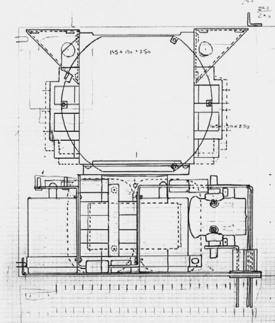
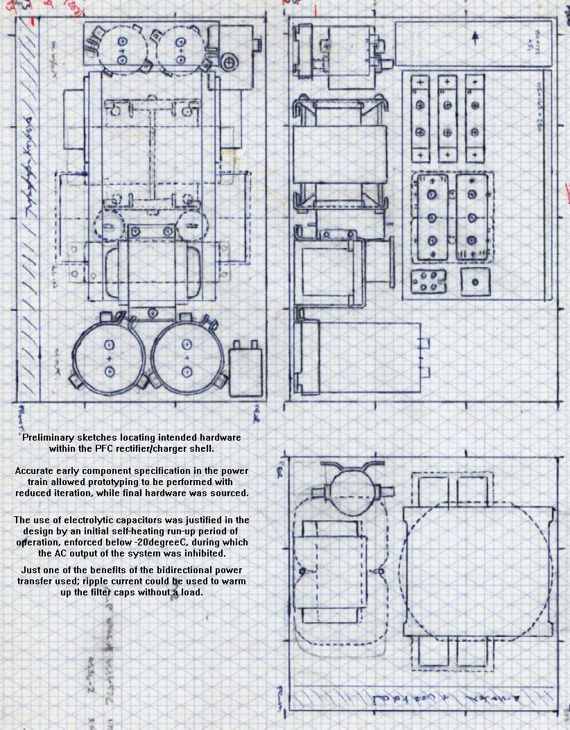
Above: End-on view of the PFC inverter, with the fab-fin power assy supported from the shell top. The fan was a 24V tubaxial version, which was switched by the PFC control assy. Copper bussbars extending below the mounting surface mated with the filter/limiter and connector subassembly.
The wide-range input, full-bridge boost converter supplied both the isolated +/- 200V bus for the Output inverter port and power for the isolated 24V battery bidirectional charging terminals. Failure of the AC supply allowed immediate back-up from battery storage, using the same transformer and semiconductor switches. When the AC input supply was present, the PbSO4 batteries were charged with surplus input energy when the inverter 120VAC output load demand fell below 3KVA.
A relay assembly, located on the HVDC output capacitor terminals, was used to sense and to optimally configure the input power train on start-up, under the control of the PFC microprocessor. This switched the PFC power circuitry over from the full bridge topology, normally present for a 240VAC input, to a push-pull topology in the 120VAC input range. Various control and measuring circuits were also configured at this time to reduce distortion and maintain noise immunity. Current density, voltage stress and duty cycle in the power semiconductors and magnetics was uniform over both operating ranges.
Conversion and power flow control was automatic in the hardware, though monitored, measured and supervised by a local microprocessor which also communicated status and signal information to the main operator control and display panel. Both the control panel and the AC output inverter were standard Exide Electronics replacable modules, with their own independant microproccessors on-board.
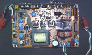
The Control circuitry in all subassemblies was powered by a separate uninterruptible supply, with multiple isolated outputs, mounted on one removable shell side wall. The functional breadboard for this converter is pictured above.
The other hinged side wall housed the PFC controller and the display/keyboard panel assemblies. If the second hinged wall was let down, the battery disconnect, power filter, output inverter module, fan and all other PFC hardware could be accessed for replacement or maintenance. Isolated drive interface circuitry for all power semiconductors was located in trays, accessible through the unit's lid.
The PFC/Charger and PWM inverter modules were in turn mounted within a welded Aluminum frame, the base of which supported another removable module, housing input and output filters, fuses, circuit breakers and I/O power socketry.
Environmental performance was confirmed over the humidity and temperature ranges. As an air-breather, the use dry ice in substitute for liquid nitrogen may have slewed low temperature performance somewhat, and also prevented controlled testing for cyclical thermal shock rate-of-change. The biggest problem was operating the device without the benefit of a functioning display - the commercial version of the control and display module sported an LCD indicator which became illegible below 0degC. This obviously complicated a user-initiated start-up at 40degC below zero, which had to be performed using a series of keystrokes from memory; both frequency and amplitude required manual input to cover the output voltage and frequency ranges specified.
EMC compliance of this device was tested at Spar Aerospace, and this was also complicated by the performance of the commercial Exide Technology modules. These both radiated to the outside world through the display/keyboard panel opening and a nearby box wall seam, until the locations were properly gasketed. Source of the noise was likely improperly specified or applied processor crystal clock modules.