It isn't very often that 'power supply guys' find themselves in
a situation where they can shoot the breeze with like-minded individuals.
When ever this happened in the 80's, I liked to bring out what I came to
think of as 'party trick' gate drive.
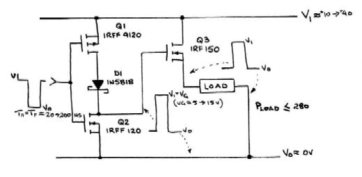
The following circuit was constructed: (out comes the pencil and paper)
Note that the input was a square wave with amplitude switching between
V1 and V0.
Q1 and Q2 were P and Nchannel mosfets, arranged as a typical inverter.
The only difference is the insertion of a schottky diode in series
wth their drains.
The voltage showing up on the gate of Q3 exceeds the V1 rail, enough to drive Q3 in an efficient manner. The full supply rail showed up across the load.
Was this magic, or what?
In reality, breadboarding commenced with an added component that does not appear in the 'trick' schematic. This was an inductor placed in series with D1. Iterations proved that this inductor was not strictly required, to obtain the original aim - which was that of using the cross-conduction parasitic current as a source for gate-drive energy. If this were possible, then cross-conduction, if properly controlled, could become a useful feature in high-frequency switching, rather than a power-wasting niusance.
In the actual event, I spent a lot of time checking scopes and adding and removing probes, trying to get the readings to make sense. I found that simply adding probe capacitance between the supply rail and the gate of Q3 actually increased the gate voltage amplitude. Fiddling with capacitors confirmed the effect. Adding local decoupling capacitors across the supply rail also had an effect.
It became obvious that I was dealing with a parasitic resonance, of a sort, so the aim became to make this work in a predictable and controlled manner.
The parasitic inductances working in favor of boosted Q3 gate voltage were those in series with D1 when cross-conduction currents flowed through Q1 and Q2. These could include supply capacitor and lead inductance strays. Placing a bead in series with Q1 and D1 confirmed this, by making the voltage on the gate of Q3 much more predictable. The peak cross-conduction current stored energy in the bead. This energy was delivered to the gate of Q3 when Q2 turned off.
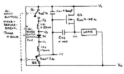
Crunching some numbers, it became apparent that this was a phenomenon that could even be employed to some advantage in integrated circuits. This is just using inductance values formed on the legs of an integrated circuit package, never mind in an IC that had an intentional internally-constructed MEMS inductor.
Cross-conduction in integrated Cmos inverters is actually hard to avoid; package lead inductance is free - a technique that uses these characteristics seems rather serendipitous. If you combine it with adiabatic techniques employing an AC clock supply, who knows what you could do?
There are stumbling blocks - scaling peak currents to capacitive loads and fabricating schottky structures may not be the most difficult of these. Anything with large peak currents can be lossy - the inductor is intended to avoid this, but is not used in the discharge of the gate, in the schematic drawn above.
A Linear Technology Switchercad III plot of the gate drive rising transition is plotted below.
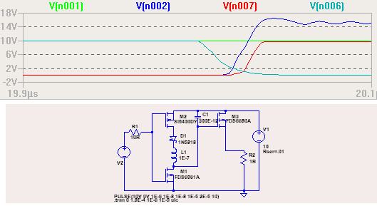
Light Blue - input drive.
Red - Load voltage = Q3source
Dark Blue - Q3gate
Green - Vcc=Q3 drain
Gate rise time is 20nSec to VCC+6V with the components and waveforms used. The text contents of the schematic file is appended to the end of this page.
Serendipity and prestidigitation aside, I used this technique in a number of lower voltage and battery-supplied motor and voice coil driver circuits. I also performed a comprehensive patent search on the technique, or anything close to it, at the time.
You can consider it as being in the public domain, and maybe even pass it on at your next rare gathering of power-circuit-whipped individuals.

LT CAD III file follows:
...........................
Version 4
SHEET 1 880 680
WIRE 64 64 192 64
WIRE 192 64 336 64
WIRE 336 64 512 64
WIRE 512 64 512 160
WIRE 512 480 512 240
WIRE 512 480 432 480
WIRE 64 480 64 448
WIRE 64 480 -192 480
WIRE -192 480 -192 320
WIRE 64 336 64 352
WIRE 64 240 64 256
WIRE 64 160 64 176
WIRE -176 176 -192 176
WIRE -192 176 -192 240
WIRE -96 176 -48 176
WIRE -48 176 -48 432
WIRE -48 432 16 432
WIRE -48 80 -48 176
WIRE -48 80 16 80
WIRE 64 352 192 352
WIRE 192 352 192 144
WIRE 288 144 192 144
WIRE 192 144 192 128
WIRE 336 160 336 272
WIRE 336 272 432 272
WIRE 432 352 432 480
WIRE 432 480 64 480
WIRE 432 496 432 480
FLAG 432 496 0
SYMBOL schottky 48 176 R0
WINDOW 0 54 18 Left 0
WINDOW 3 42 50 Left 0
SYMATTR InstName D1
SYMATTR Value 1N5818
SYMATTR Description Diode
SYMATTR Type diode
SYMBOL ind 48 240 R0
WINDOW 0 58 38 Left 0
WINDOW 3 48 70 Left 0
SYMATTR InstName L1
SYMATTR Value 1E-7
SYMBOL cap 176 64 R0
WINDOW 0 42 18 Left 0
WINDOW 3 23 53 Left 0
SYMATTR InstName C1
SYMATTR Value 300E-12
SYMBOL res -80 160 R90
WINDOW 0 0 56 VBottom 0
WINDOW 3 32 56 VTop 0
SYMATTR InstName R1
SYMATTR Value 10R
SYMBOL nmos 16 352 R0
WINDOW 0 87 27 Left 0
WINDOW 3 57 56 Left 0
SYMATTR InstName M1
SYMATTR Value FDS6961A
SYMBOL pmos 16 160 M180
WINDOW 0 82 68 Left 0
WINDOW 3 53 40 Left 0
SYMATTR InstName M2
SYMATTR Value Si9400DY
SYMBOL nmos 288 64 R0
WINDOW 0 84 28 Left 0
WINDOW 3 53 53 Left 0
SYMATTR InstName M3
SYMATTR Value FDS6680A
SYMBOL res 416 256 R0
WINDOW 0 45 40 Left 0
WINDOW 3 48 71 Left 0
SYMATTR InstName R2
SYMATTR Value 1R
SYMBOL voltage 512 144 R0
WINDOW 123 0 0 Left 0
WINDOW 39 24 132 Left 0
SYMATTR InstName V1
SYMATTR Value 10
SYMATTR SpiceLine Rser=.01
SYMBOL voltage -192 224 R0
WINDOW 0 -36 112 Left 0
WINDOW 3 -52 285 Left 0
WINDOW 123 0 0 Left 0
WINDOW 39 0 0 Left 0
SYMATTR InstName V2
SYMATTR Value PULSE(10V 0V 1E-6 1E-8 1E-8 1E-5 2E-5 10)
TEXT -246 530 Left 0 !.tran 0 1.8E-4 1E-6 1E-9 uic
............................................
Simply create a text file using contents between the dotted lines
and rename the file extension as .asc to run as an LT SwitcherCad III pspice
schematic file.