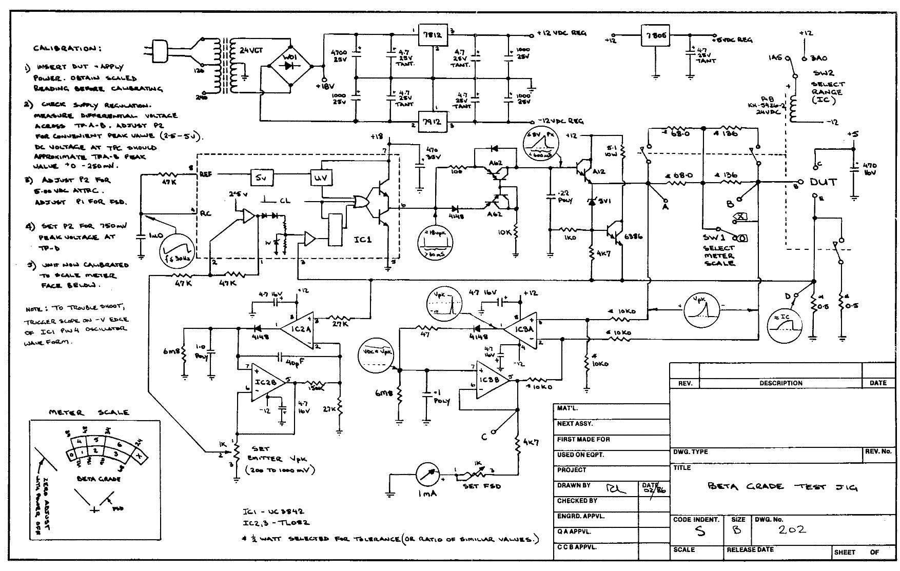
The original GFC linear power power supplies used a current measurement and limiting circuit that was originally intended for lower power, low voltage applications. This monitored the base current of the pass transistors. Unfortunately it was also misapplied in higher power and higher voltage applications, without taking the precaution of limiting or controlling in some way, the variations of beta that typical power transistors can exhibit.
This meant that paralleled devices did not share predictably, nor was the dissipation of higher voltage units very carefully controlled. An original jig, designed to allow grading of devices using hardware in a 4-foot-tall,19-inch rack, merely succeeded in burning operator fingers and damaging the DUTs.
I offered the following circuit, built into a portable, bright-yellow plastic box.
This had the advantage (besides being small and portable) that it didn't overstress the DUT or the operator's fingers and gave unambiguous part grades that could be directed towards suitable linear applications. Lower beta parts were naturally steered towards lower current, higher voltage applications. A press-fit socket allowed quick manual insertion and removal.
Internally, collector voltage was maintained at an approximately constant 5V (-Ve) with a low average current limit. Base current was periodically ramped up from zero to generate emitter current at one of two preset levels common to the linear regulator application circuit limit (1.5 or 3A). Peak base current was detected and displayed on an analog meter, which could be calibrated in hfe - beta reducing with increased deflection. Units failing to grade within useful limits could be scrapped or used in non-critical applications, internally.
The current range was controlled by the front panel range which energized hermetic relay contacts. Ideally the collector voltage should also have included a lower range of collector voltage, to weed out VCEsat-induced errors, but the coincidental occurance of drop-out and overload was expected to produce results that were both within specification and non-damaging to the circuitry.
This is an application of the 3842 IC that isn't seen very often. Full calibration procedure is noted on the original schematic (which should be conveniently fastened to the inside of the tester box lid).
A full-scale (1mA) meter panel sketch is available here.